
ਇੱਕ ਗਲੋਬਲ ਦੇ ਰੂਪ ਵਿੱਚ ਕਸਟਮ ਕੱਚ ਨਿਰਮਾਤਾ, ਅਸੀਂ ਪ੍ਰਦਾਨ ਕਰਨ ਵਿੱਚ ਮਾਹਰ ਹਾਂ ਉੱਚ-ਸ਼ੁੱਧਤਾ ਵਾਲੇ ਕੱਚ ਦੇ ਪਦਾਰਥ ਅਤੇ ਵਿਸ਼ੇਸ਼ ਪ੍ਰੋਸੈਸਿੰਗ ਸੇਵਾਵਾਂ ਸਭ ਤੋਂ ਵੱਧ ਮੰਗ ਵਾਲੇ ਉਦਯੋਗਾਂ ਲਈ ਤਿਆਰ ਕੀਤਾ ਗਿਆ - ਸਮੇਤ ਜੈਵਿਕ ਸੈਮੀਕੰਡਕਟਰ, MEMS, AR/VR ਆਪਟਿਕਸ, ਮੈਡੀਕਲ ਡਾਇਗਨੌਸਟਿਕਸਹੈ, ਅਤੇ ਅਕਾਦਮਿਕ ਖੋਜ. ਸਾਡੇ ਉਤਪਾਦਾਂ 'ਤੇ ਦੁਨੀਆ ਭਰ ਦੀਆਂ ਪ੍ਰਮੁੱਖ ਪ੍ਰਯੋਗਸ਼ਾਲਾਵਾਂ ਅਤੇ ਸੰਸਥਾਵਾਂ ਦੁਆਰਾ ਭਰੋਸਾ ਕੀਤਾ ਗਿਆ ਹੈ।
ਅਸੀਂ ਉੱਨਤ ਖੋਜਕਰਤਾਵਾਂ ਲਈ ਮਾਣ ਨਾਲ ਹੱਲ ਪ੍ਰਦਾਨ ਕਰਦੇ ਹਾਂ ਸੈਂਟਰ ਕੱਟਆਊਟਸ ਵਾਲੀਆਂ ਕੱਚ ਦੀਆਂ ਕਵਰ ਪਲੇਟਾਂ, ਕਿਨਾਰੇ ਵਾਲੇ ਕਦਮਹੈ, ਅਤੇ ਆਪਟੀਕਲ-ਪੱਧਰੀ ਸਤਹ ਸਮਾਪਤੀ, ਸਹੀ ਡਿਜ਼ਾਈਨ ਅਤੇ ਐਪਲੀਕੇਸ਼ਨ-ਵਿਸ਼ੇਸ਼ ਮਾਪਦੰਡਾਂ ਨੂੰ ਪੂਰਾ ਕਰਦੇ ਹੋਏ।
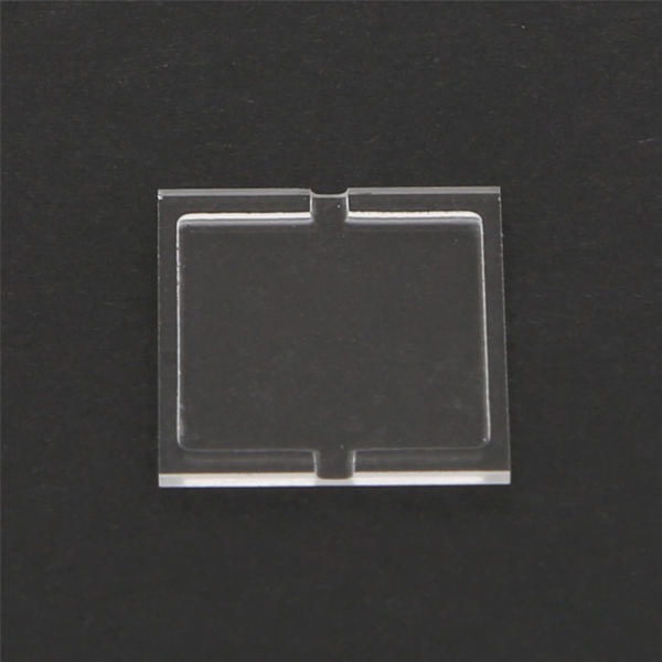
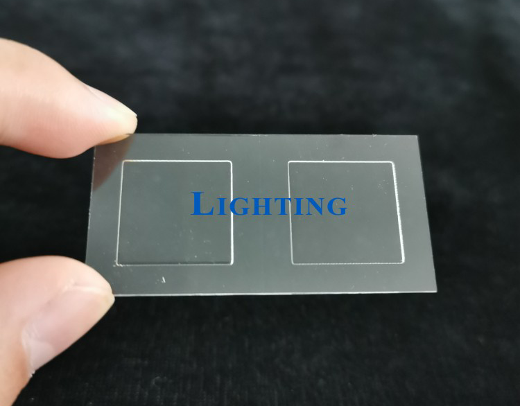
ਕੇਂਦਰੀ ਖੁੱਲਣ ਅਤੇ ਕਿਨਾਰੇ ਵਾਲੇ ਕਦਮਾਂ ਵਾਲੀ ਕਸਟਮ ਕੱਚ ਦੀ ਕਵਰ ਪਲੇਟ
ਸਾਡੇ ਵੱਲੋਂ ਅਕਸਰ ਮੰਗੀਆਂ ਜਾਣ ਵਾਲੀਆਂ ਉਤਪਾਦ ਲਾਈਨਾਂ ਵਿੱਚੋਂ ਇੱਕ ਵਿੱਚ ਵੱਖ-ਵੱਖ ਉੱਨਤ ਐਪਲੀਕੇਸ਼ਨਾਂ ਲਈ ਕਸਟਮ ਗਲਾਸ ਕਵਰ ਸ਼ਾਮਲ ਹਨ। ਇਹਨਾਂ ਵਿੱਚ ਬੰਧਨ ਅਤੇ ਸੀਲਿੰਗ ਲਈ ਸਟੀਕ ਕੱਟੇ ਹੋਏ ਸੈਂਟਰ ਕੈਵਿਟੀਜ਼ ਅਤੇ ਸਟੈਪਡ ਕਿਨਾਰਿਆਂ ਵਾਲੇ ਐਨਕੈਪਸੂਲੇਸ਼ਨ ਕਵਰ, ਨਾਲ ਹੀ ਸੁਰੱਖਿਆ ਵਾਲੇ ਸ਼ੀਸ਼ੇ ਦੀਆਂ ਖਿੜਕੀਆਂ, ਮਾਈਕ੍ਰੋਫਲੂਇਡਿਕ ਡਿਵਾਈਸਾਂ ਲਈ ਪਾਰਦਰਸ਼ੀ ਕਵਰ, ਅਤੇ ਬੰਧਨ ਜਾਂ ਆਪਟੀਕਲ ਅਲਾਈਨਮੈਂਟ ਲਈ ਸਬਸਟਰੇਟ ਸ਼ਾਮਲ ਹਨ। ਭਾਵੇਂ ਜੈਵਿਕ ਸੈਮੀਕੰਡਕਟਰ ਡਿਵਾਈਸਾਂ ਦੀ ਰੱਖਿਆ ਕਰਨ, MEMS ਢਾਂਚਿਆਂ ਦਾ ਸਮਰਥਨ ਕਰਨ, ਜਾਂ ਪਤਲੇ-ਫਿਲਮ ਸੈਂਸਰਾਂ ਨੂੰ ਸੀਲ ਕਰਨ ਲਈ ਵਰਤਿਆ ਜਾਂਦਾ ਹੈ, ਸਾਡੇ ਹਿੱਸੇ ਕਠੋਰ ਵਾਤਾਵਰਣਾਂ ਵਿੱਚ ਭਰੋਸੇਯੋਗ ਢੰਗ ਨਾਲ ਕੰਮ ਕਰ ਸਕਦੇ ਹਨ।
ਸਾਡੀਆਂ ਸਮਰੱਥਾਵਾਂ ਵਿੱਚ ਸ਼ਾਮਲ ਹਨ:
- ਸੀ ਐਨ ਸੀ ਮਿਲਿੰਗ ਸਖ਼ਤ ਸਹਿਣਸ਼ੀਲਤਾ ਨਿਯੰਤਰਣ ਵਾਲੇ ਗੋਲਾਕਾਰ ਜਾਂ ਆਇਤਾਕਾਰ ਖੁੱਲਣ ਦਾ
- ਐਜ ਸਟੈਪ ਮਸ਼ੀਨਿੰਗ ਚਿਪਕਣ ਵਾਲੀ ਬੰਧਨ ਜਾਂ ਦਬਾਅ ਸੀਲਿੰਗ ਲਈ
- ਅਤਿ-ਨਿਰਵਿਘਨ ਸਤਹਾਂ ਆਪਟੀਕਲ ਪਾਰਦਰਸ਼ਤਾ ਲਈ Ra < 5 Å ਤੱਕ ਪਾਲਿਸ਼ ਕੀਤਾ ਗਿਆ
- ਅਯਾਮੀ ਇਕਸਾਰਤਾ ±0.01 ਮਿਲੀਮੀਟਰ ਦੇ ਅੰਦਰ, ਛੋਟੇ ਬੈਚਾਂ ਲਈ ਵੀ
ਇਹ ਵਿਸ਼ੇਸ਼ਤਾਵਾਂ ਸਾਡੇ ਖੋਜ ਪੈਕੇਜਿੰਗ ਐਪਲੀਕੇਸ਼ਨਾਂ ਲਈ ਆਦਰਸ਼ ਕੱਚ ਦੇ ਸਬਸਟਰੇਟ ਜਿੱਥੇ ਮਕੈਨੀਕਲ ਫਿੱਟ ਅਤੇ ਸਤ੍ਹਾ ਦੀ ਗੁਣਵੱਤਾ ਦੋਵੇਂ ਸਿੱਧੇ ਤੌਰ 'ਤੇ ਡਿਵਾਈਸ ਦੀ ਇਕਸਾਰਤਾ ਅਤੇ ਟੈਸਟ ਵੈਧਤਾ ਨੂੰ ਪ੍ਰਭਾਵਿਤ ਕਰਦੇ ਹਨ।
ਖੋਜ-ਅਧਾਰਤ ਐਪਲੀਕੇਸ਼ਨਾਂ ਲਈ ਤਿਆਰ ਕੀਤੇ ਗਏ ਗਲਾਸ ਸਮਾਧਾਨ
ਅਸੀਂ ਵਿਆਪਕ ਤੌਰ 'ਤੇ ਕੰਮ ਕਰਦੇ ਹਾਂ ਵਿਗਿਆਨਕ ਪ੍ਰਯੋਗਸ਼ਾਲਾਵਾਂ, ਯੂਨੀਵਰਸਿਟੀ ਵਿਭਾਗਹੈ, ਅਤੇ ਆਰ ਐਂਡ ਡੀ ਟੀਮਾਂ ਜੈਵਿਕ ਸੈਮੀਕੰਡਕਟਰ ਪੈਕੇਜਿੰਗ, OLED ਡਿਸਪਲੇ, ਅਤੇ ਅਗਲੀ ਪੀੜ੍ਹੀ ਦੇ ਸੈਂਸਰਾਂ ਵਾਲੇ ਪ੍ਰੋਜੈਕਟਾਂ 'ਤੇ। ਸਾਡੇ ਉਤਪਾਦਾਂ ਨੂੰ ਇਹਨਾਂ ਵਿੱਚ ਲਾਗੂ ਕੀਤਾ ਗਿਆ ਹੈ:
- ਜੈਵਿਕ ਫੋਟੋਵੋਲਟੇਇਕ ਇਨਕੈਪਸੂਲੇਸ਼ਨ
- ਲਚਕਦਾਰ ਟਰਾਂਜ਼ਿਸਟਰ ਪੈਕੇਜਿੰਗ
- ਵੇਫਰ-ਪੱਧਰ MEMS ਸੁਰੱਖਿਆ
- ਫੋਟੋਨਿਕ ਪ੍ਰਯੋਗਾਂ ਲਈ ਕੱਚ ਦੇ ਕਵਰ
- ਮਾਈਕ੍ਰੋਫਲੂਇਡਿਕ ਚਿੱਪ ਸੀਲਿੰਗ
ਸਾਡੇ ਇੰਜੀਨੀਅਰ ਇਸ ਵਿੱਚ ਮਾਹਰ ਹਨ ਖੋਜ ਭਾਸ਼ਾ ਅਤੇ ਪ੍ਰਯੋਗਾਤਮਕ ਜ਼ਰੂਰਤਾਂ. ਭਾਵੇਂ ਤੁਹਾਡਾ ਡਿਜ਼ਾਈਨ CAD ਵਿੱਚ ਹੋਵੇ, ਹੱਥ ਨਾਲ ਬਣਾਇਆ ਸਕੈਚ ਹੋਵੇ, ਜਾਂ ਸਿਰਫ਼ ਇੱਕ ਕਾਰਜਸ਼ੀਲ ਲੋੜ ਹੋਵੇ, ਅਸੀਂ ਇਸਨੂੰ ਇੱਕ ਨਿਰਮਾਣਯੋਗ ਕੱਚ ਦੇ ਹਿੱਸੇ ਵਿੱਚ ਅਨੁਵਾਦ ਕਰਨ ਵਿੱਚ ਮਦਦ ਕਰਾਂਗੇ — ਤੇਜ਼ ਅਤੇ ਭਰੋਸੇਯੋਗ ਢੰਗ ਨਾਲ।
ਸ਼ੁੱਧਤਾ ਸੀਐਨਸੀ ਗਲਾਸ ਮਸ਼ੀਨਿੰਗ ਵਿਗਿਆਨਕ ਵਰਤੋਂ ਲਈ
ਸਾਡੀਆਂ ਉੱਨਤ CNC ਮਸ਼ੀਨਿੰਗ ਸਮਰੱਥਾਵਾਂ ਸਾਨੂੰ ਸਭ ਤੋਂ ਗੁੰਝਲਦਾਰ ਡਿਵਾਈਸ ਹਾਊਸਿੰਗ ਢਾਂਚਿਆਂ ਲਈ ਵੀ ਕਸਟਮ ਜਿਓਮੈਟਰੀ ਪ੍ਰਦਾਨ ਕਰਨ ਦੀ ਆਗਿਆ ਦਿੰਦੀਆਂ ਹਨ। ਅਸੀਂ ਇਹ ਪ੍ਰਾਪਤ ਕਰ ਸਕਦੇ ਹਾਂ:
| ਪੈਰਾਮੀਟਰ | ਸਮਰੱਥਾ |
|---|---|
| ਘੱਟੋ-ਘੱਟ ਮੋਟਾਈ | 0.10 ਮਿਲੀਮੀਟਰ |
| ਅਧਿਕਤਮ ਆਕਾਰ | 600 ਮਿਲੀਮੀਟਰ × 600 ਮਿਲੀਮੀਟਰ |
| ਕੇਂਦਰੀ ਕੱਟਆਉਟ ਸਹਿਣਸ਼ੀਲਤਾ | ± 0.02 ਮਿਲੀਮੀਟਰ |
| ਕਦਮ ਡੂੰਘਾਈ / ਕਿਨਾਰੇ ਦੀ ਵਿਸ਼ੇਸ਼ਤਾ | ±0.01 ਮਿਲੀਮੀਟਰ ਸ਼ੁੱਧਤਾ |
| ਸਤਹ ਖੁਰਦਰੀ (Ra) | 5 Å (0.5 nm) ਤੱਕ ਘੱਟ |
| ਕਲੀਨਰੂਮ ਅਨੁਕੂਲਤਾ | ਕਲਾਸ 1000 (ISO 5) ਅਲਟਰਾਸੋਨਿਕ ਸਫਾਈ ਅਤੇ ਵੈਕਿਊਮ ਪੈਕੇਜਿੰਗ |
ਇਹ ਸਮਰੱਥਾਵਾਂ ਸਾਨੂੰ ਇੱਕ ਪਸੰਦੀਦਾ ਭਾਈਵਾਲ ਬਣਾਉਂਦੀਆਂ ਹਨ ਆਪਟੀਕਲ ਵੇਫਰ ਪਾਲਿਸ਼ਿੰਗ, ਕੱਚ ਦੇ ਕਵਰ ਮਾਈਕ੍ਰੋ-ਮਸ਼ੀਨਿੰਗਹੈ, ਅਤੇ ਐਨਕੈਪਸੂਲੇਸ਼ਨ ਗਲਾਸ ਨਿਰਮਾਣ ਵਿਗਿਆਨਕ ਅਤੇ ਪ੍ਰਯੋਗਾਤਮਕ ਉਪਯੋਗਾਂ ਲਈ।
ਦੁਨੀਆ ਭਰ ਦੇ ਖੋਜਕਰਤਾ ਸਾਡੇ 'ਤੇ ਕਿਉਂ ਭਰੋਸਾ ਕਰਦੇ ਹਨ
ਸਾਡੀ ਕੰਪਨੀ ਸਿਰਫ਼ ਇੱਕ ਕੱਚ ਦੀ ਫੈਕਟਰੀ ਨਹੀਂ ਹੈ - ਅਸੀਂ ਇੱਕ ਹਾਂ ਹੱਲ ਸਾਥੀ ਖੋਜਕਰਤਾਵਾਂ ਨੂੰ। ਅਸੀਂ ਸਮਝਦੇ ਹਾਂ:
ਅਸੀਂ ਜਰਮਨੀ, ਫਰਾਂਸ, ਅਮਰੀਕਾ, ਕੋਰੀਆ, ਅਤੇ ਇਸ ਤੋਂ ਬਾਹਰ ਦੇ ਸੰਸਥਾਨਾਂ ਨੂੰ ਸਫਲਤਾਪੂਰਵਕ ਕਸਟਮ ਕਵਰ ਪਲੇਟ ਹੱਲ ਪ੍ਰਦਾਨ ਕੀਤੇ ਹਨ। ਸਾਡੀ ਕਲਾਇੰਟ ਸੂਚੀ ਵਿੱਚ ਸਰਕਾਰ ਦੁਆਰਾ ਫੰਡ ਪ੍ਰਾਪਤ ਪ੍ਰਯੋਗਸ਼ਾਲਾਵਾਂ, ਸੈਮੀਕੰਡਕਟਰ ਖੋਜ ਕੇਂਦਰ, ਅਤੇ ਅੰਤਰ-ਅਨੁਸ਼ਾਸਨੀ ਇੰਜੀਨੀਅਰਿੰਗ ਟੀਮਾਂ ਸ਼ਾਮਲ ਹਨ।
ਆਰਗੈਨਿਕ ਸੈਮੀਕੰਡਕਟਰ ਪੈਕੇਜਿੰਗ ਲਈ ਕਸਟਮ ਗਲਾਸ
ਜੈਵਿਕ ਸੈਮੀਕੰਡਕਟਰ ਯੰਤਰਾਂ ਦੀ ਪੈਕੇਜਿੰਗ ਲਈ ਸਟੀਕ, ਅਟੱਲ ਅਤੇ ਸਥਿਰ ਸਮੱਗਰੀ ਦੀ ਲੋੜ ਹੁੰਦੀ ਹੈ ਜੋ ਆਪਟੀਕਲ ਜਾਂ ਇਲੈਕਟ੍ਰੀਕਲ ਵਿਸ਼ੇਸ਼ਤਾਵਾਂ ਵਿੱਚ ਦਖਲ ਨਹੀਂ ਦਿੰਦੀਆਂ। ਅਸੀਂ ਤੁਹਾਨੂੰ ਇਹ ਪੇਸ਼ਕਸ਼ ਕਰ ਸਕਦੇ ਹਾਂ:
- ਗੈਸ ਛੱਡੇ ਬਿਨਾਂ ਇਨਰਟ ਇਨਕੈਪਸੂਲੇਸ਼ਨ
- ਬਹੁਤ ਜ਼ਿਆਦਾ ਅਨੁਕੂਲਿਤ ਕਿਨਾਰੇ ਪ੍ਰੋਫਾਈਲ ਗਲੂਇੰਗ, ਪ੍ਰੈਸ਼ਰ ਫਿਟਿੰਗ, ਜਾਂ ਥਰਮਲ ਬਾਂਡਿੰਗ ਲਈ
- ਕੱਟਆਊਟ ਵਿੰਡੋਜ਼ ਸਰਗਰਮ ਪਰਤਾਂ ਨਾਲ ਦਖਲਅੰਦਾਜ਼ੀ ਨੂੰ ਰੋਕਣ ਲਈ
- ਪਰਤ ਅਨੁਕੂਲਤਾ ਜੇ ਲੋੜ ਹੋਵੇ ਤਾਂ AR ਜਾਂ ਹਾਈਡ੍ਰੋਫੋਬਿਕ ਫਿਨਿਸ਼ ਲਈ
ਇਹ ਗੁਣ ਸਾਡੀਆਂ ਕੱਚ ਦੀਆਂ ਪਲੇਟਾਂ ਨੂੰ ਖੋਜ ਲਈ ਆਦਰਸ਼ ਬਣਾਉਂਦੇ ਹਨ ਜੈਵਿਕ ਫੀਲਡ-ਇਫੈਕਟ ਟਰਾਂਜ਼ਿਸਟਰ (OFETs), ਆਰਗੈਨਿਕ ਰੋਸ਼ਨੀ-ਇਮੀਟਿੰਗ ਡਾਇਡਸ (OLEDs), ਪਤਲੀ-ਫਿਲਮ ਇਨਕੈਪਸੂਲੇਸ਼ਨ, ਅਤੇ ਹੋਰ.
ਇੱਕ ਡਰਾਇੰਗ ਨਾਲ ਸ਼ੁਰੂ ਕਰੋ, ਇੱਕ ਹੱਲ ਨਾਲ ਖਤਮ ਕਰੋ
ਭਾਵੇਂ ਤੁਸੀਂ ਆਪਣੀ ਪਹਿਲੀ ਪ੍ਰਯੋਗਾਤਮਕ ਦੌੜ ਦੀ ਤਿਆਰੀ ਕਰ ਰਹੇ ਹੋ ਜਾਂ ਇੱਕ ਮਹੱਤਵਪੂਰਨ ਲੰਬੇ ਸਮੇਂ ਦੇ ਟੈਸਟ ਨੂੰ ਅਨੁਕੂਲ ਬਣਾ ਰਹੇ ਹੋ, ਅਸੀਂ ਖੋਜ ਸਮੂਹਾਂ ਨੂੰ ਵਿਚਾਰ ਤੋਂ ਹਾਰਡਵੇਅਰ ਵੱਲ ਤੇਜ਼ੀ ਨਾਲ ਅੱਗੇ ਵਧਣ ਵਿੱਚ ਮਦਦ ਕਰਦੇ ਹਾਂ। ਸਾਡੇ ਤਕਨੀਕੀ ਵਿਕਰੀ ਇੰਜੀਨੀਅਰ ਤੁਹਾਡੀ ਟੀਮ ਨਾਲ ਮਿਲ ਕੇ ਕੰਮ ਕਰਦੇ ਹਨ:
- ਡਰਾਇੰਗਾਂ ਜਾਂ ਸਕੈਚਾਂ ਦੀ ਸਮੀਖਿਆ ਕਰੋ
- ਸਮੱਗਰੀ, ਸਹਿਣਸ਼ੀਲਤਾ, ਅਤੇ ਸਮਾਪਤੀ ਬਾਰੇ ਸੁਝਾਅ ਦਿਓ।
- ਜਲਦੀ ਹਵਾਲੇ ਪ੍ਰਦਾਨ ਕਰੋ (24-48 ਘੰਟਿਆਂ ਦੇ ਅੰਦਰ)
- ਸਕੇਲ-ਅੱਪ ਅਤੇ ਪ੍ਰਕਾਸ਼ਨ ਲਈ ਦੁਹਰਾਉਣ ਯੋਗ ਨਤੀਜੇ ਯਕੀਨੀ ਬਣਾਓ।
ਉੱਥੇ ਹੈ ਕੋਈ ਘੱਟੋ-ਘੱਟ ਆਰਡਰ ਮਾਤਰਾ ਨਹੀਂ, ਅਤੇ ਅਸੀਂ ਅਨੁਕੂਲਤਾ ਪ੍ਰਦਾਨ ਕਰਦੇ ਹਾਂ ਕਈ ਡਿਜ਼ਾਈਨ ਦੁਹਰਾਓ ਬਿਨਾਂ ਦੇਰੀ ਕੀਤੇ.
ਕੱਚ ਦੀ ਸਤ੍ਹਾ ਦੀ ਸਮਾਪਤੀ ਅਤੇ ਪਾਲਿਸ਼ਿੰਗ ਸੇਵਾਵਾਂ
ਜਿਓਮੈਟ੍ਰਿਕ ਪ੍ਰੋਸੈਸਿੰਗ ਤੋਂ ਇਲਾਵਾ, ਅਸੀਂ ਪੇਸ਼ ਕਰਦੇ ਹਾਂ ਸ਼ੁੱਧਤਾ ਵਾਲੇ ਸ਼ੀਸ਼ੇ ਦੀ ਲੈਪਿੰਗ ਅਤੇ ਪਾਲਿਸ਼ਿੰਗ ਸੇਵਾਵਾਂ ਅਤਿ-ਫਲੈਟ, ਬੰਧਨ-ਗ੍ਰੇਡ ਵਿਸ਼ੇਸ਼ਤਾਵਾਂ ਨੂੰ ਪੂਰਾ ਕਰਨ ਲਈ। ਲੋੜੀਂਦਾ ਐਪਲੀਕੇਸ਼ਨਾਂ ਲਈ ਆਪਟੀਕਲ ਵੇਫਰ ਪਾਲਿਸ਼ਿੰਗ, ਸਾਫ਼-ਸਫ਼ਾਈ-ਗ੍ਰੇਡ ਸਤ੍ਹਾ ਦੀ ਤਿਆਰੀ, ਜ ਸਮਤਲਤਾ ਅਤੇ ਸਮਾਨਤਾ ਵਾਲਾ ਸ਼ੀਸ਼ਾ ਮਲਟੀ-ਲੇਅਰ ਸਟੈਕਾਂ ਵਿੱਚ ਮੇਲ ਖਾਂਦੇ ਹੋਏ, ਅਸੀਂ ਪੇਸ਼ ਕਰਦੇ ਹਾਂ:
- ਇਕਸਾਰਤਾ ਲਈ ਦੋ-ਪਾਸੜ ਪਾਲਿਸ਼ਿੰਗ
- ਮੋਟਾਈ ਸਹਿਣਸ਼ੀਲਤਾ ±0.005 ਮਿਲੀਮੀਟਰ ਤੱਕ
- ਲੇਜ਼ਰ ਅਲਾਈਨਮੈਂਟ ਜਾਂ ਬਾਂਡਿੰਗ ਲਈ λ/10 ਤੱਕ ਸਮਤਲਤਾ
- ਕਿਨਾਰੇ ਦੀ ਚੈਂਫਰਿੰਗ ਅਤੇ ਸੁਰੱਖਿਆ ਪੈਕੇਜਿੰਗ
ਸਾਡਾ ਕੱਚ ਦੀ ਸਤ੍ਹਾ ਦੀ ਸਮਾਪਤੀ ਪ੍ਰਕਿਰਿਆਵਾਂ ਸੀਲਿੰਗ ਭਰੋਸੇਯੋਗਤਾ ਨੂੰ ਵਧਾਉਂਦੀਆਂ ਹਨ, ਕਣਾਂ ਦੀ ਗੰਦਗੀ ਨੂੰ ਘਟਾਉਂਦੀਆਂ ਹਨ, ਅਤੇ ਡਿਵਾਈਸ-ਪੱਧਰ ਦੀ ਖੋਜ ਵਿੱਚ ਲੋੜੀਂਦੀ ਸ਼ੁੱਧਤਾ ਪ੍ਰਦਾਨ ਕਰਦੀਆਂ ਹਨ।
ਨਵੀਨਤਾ ਲਈ ਤਿਆਰ ਕੀਤੇ ਗਏ ਕੱਚ ਦੇ ਸਬਸਟਰੇਟ
ਭਾਵੇਂ ਤੁਸੀਂ ਇੱਕ ਵਿਕਸਤ ਕਰ ਰਹੇ ਹੋ ਚਿੱਪ-ਸਕੇਲ OLED, ਇੱਕ ਸੀਲਬੰਦ ਮਾਈਕ੍ਰੋਫਲੂਇਡਿਕ ਸੈਂਸਰ, ਜਾਂ ਇੱਕ ਮਲਟੀ-ਲੇਅਰ ਹਾਈਬ੍ਰਿਡ ਸਟੈਕ, ਅਸੀਂ ਤੁਹਾਨੂੰ ਲੋੜੀਂਦਾ ਗਲਾਸ ਇੰਟਰਫੇਸ ਬਣਾ ਸਕਦੇ ਹਾਂ — ਸਹੀ, ਤੇਜ਼ੀ ਨਾਲ, ਅਤੇ ਸੰਚਾਰ ਅਤੇ ਸਮੱਗਰੀ ਦੋਵਾਂ ਵਿੱਚ ਪੂਰੀ ਪਾਰਦਰਸ਼ਤਾ ਨਾਲ।
ਅੱਜ ਇੱਕ ਹਵਾਲੇ ਲਈ ਬੇਨਤੀ ਕਰੋ
ਜੇ ਤੁਸੀਂ ਏ ਸੈਂਟਰ ਕਟਆਉਟ ਅਤੇ ਐਡਹਿਸਿਵ ਸਟੈਪ ਦੇ ਨਾਲ ਕਸਟਮ ਗਲਾਸ ਕਵਰ ਪਲੇਟ, ਜਾਂ ਕਿਸੇ ਵੀ ਕਿਸਮ ਦਾ ਰਿਸਰਚ-ਗ੍ਰੇਡ ਐਨਕੈਪਸੂਲੇਸ਼ਨ ਗਲਾਸ, ਅੱਜ ਹੀ ਸਾਡੇ ਨਾਲ ਸੰਪਰਕ ਕਰੋ। ਤੁਸੀਂ ਆਪਣੀ ਡਰਾਇੰਗ, ਸਕੈਚ, ਜਾਂ ਹਵਾਲਾ ਫੋਟੋ ਅਪਲੋਡ ਕਰ ਸਕਦੇ ਹੋ — ਅਤੇ ਅਸੀਂ ਇੱਕ ਵਿਸਤ੍ਰਿਤ ਹਵਾਲੇ ਅਤੇ ਸਮਾਂ-ਰੇਖਾ ਦੇ ਨਾਲ ਜਵਾਬ ਦੇਵਾਂਗੇ।
ਅਸੀਂ ਦੁਨੀਆ ਭਰ ਦੇ ਗਾਹਕਾਂ ਨੂੰ ਤੇਜ਼ ਸ਼ਿਪਿੰਗ, ਤਕਨੀਕੀ ਜਵਾਬਦੇਹੀ, ਅਤੇ ਸ਼ੁੱਧਤਾ ਨਾਲ ਸੇਵਾ ਦਿੰਦੇ ਹਾਂ ਜੋ ਸਿਰਫ਼ ਇੱਕ ਮਾਹਰ ਹੀ ਪੇਸ਼ ਕਰ ਸਕਦਾ ਹੈ।
ਆਓ ਤੁਹਾਡੇ ਪ੍ਰਯੋਗ ਨੂੰ ਜੀਵਨ ਵਿੱਚ ਲਿਆਈਏ — ਫਿੱਟ ਬੈਠਣ ਵਾਲੇ ਕੱਚ ਨਾਲ।