
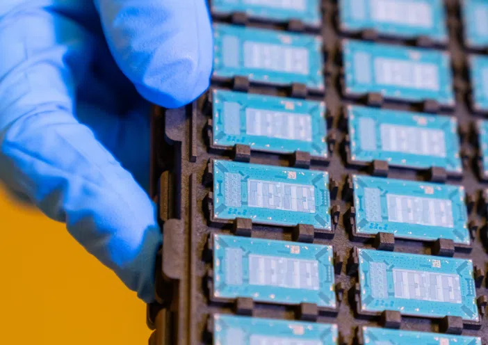
In its exploration of advanced packaging, Intel has turned its attention to a new material for chip substrates: glass. The rigidity of glass, along with its lower thermal expansion coefficient, makes it superior to organic substrates, as it reduces the degree of expansion and warping. According to Pooya Tadayon, Intel Fellow and Director of Packaging and Test Technology Development, these properties give glass a particular advantage in process scaling, such as achieving finer pitches.

Tom Rucker, Vice President of Technology Development and Director of Packaging and Test Technology Development Integration at Intel
“Using glass substrates allows us to introduce some interesting functionalities and geometries to improve power delivery,” Tadayon said. “This material can also enable high-speed diodes that go beyond 224G and even reach 448G.” He added that the adoption of glass substrates is a gradual process, driven by the development of tools and processes, as well as emerging demand. Glass substrates will coexist with organic substrates rather than replace them.
Tom Rucker, Vice President of Technology Development and Director of Packaging and Test Technology Development Integration at Intel, noted that the company has shifted its focus in advanced packaging from system-on-chip (SoC) to system-in-package (SiP).
“As we transition many of our product lines to use Embedded Multi-die Interconnect Bridge (EMIB) technology, this shift continues to gain momentum,” Rucker said. “We are also moving toward 3D interconnects, which support die stacking and allow for an increased number of dies, enabling smaller geometries and higher performance—all within a single package.”

Pooya Tadayon, Intel Fellow, Packaging and Testing Technology Development Director
The mechanical challenges posed by large-scale packaging have also prompted Intel to expand its capabilities in this area. Tadayon pointed out that substrates are prone to warping, and Mark Gardner, Senior Director of Advanced Packaging at Intel Foundry Services, added that this makes mounting them onto motherboards difficult. “As a result, we’ve found that having expertise in board assembly can be beneficial to our customers, and we can collaborate with board assembly manufacturers to provide a seamless process for them,” Gardner explained.
Driving Continuous Innovation in Packaging Technology
Intel’s newly launched and upcoming products include:
- The Max Series data center GPUs, introduced earlier in 2023, leverage nearly all of Intel’s advanced packaging technologies, including side-by-side 3D stacking and EMIB. These components contain 47 5nm process dies and 100 billion transistors.
- The next-generation 36µm pitch Foveros 3D stacking technology (which has evolved from 50µm to 36µm and now to 25µm), as well as the Meteor Lake processors, expected to launch in 2023.
- The Flip-Chip Ball-Grid-Array (FCBGA) platform, targeting mass production in 2024, plans to expand side-by-side package sizes to 100mm, extend middle layers, and reduce pitches to below 90µm.
- Next-generation interconnects, including glass-based coupling—also known as glass bridge technology—and co-packaged optics with integrated waveguides.
Tadayon explained that glass bridge technology does not directly connect or bond optical fibers to silicon chips to avoid reprocessing. This “unique solution” supports plug-and-play functionality and is expected to enter mass production by the end of 2024. Additionally, Intel’s Foveros chip stacking technology will continue to evolve, with pitches expected to shrink to 9µm.
“Looking ahead to next-generation technologies, we plan to adopt pitches below 5µm in our products,” Tadayon said. “We will continue to introduce novel architectures and 3D stacking capabilities, allowing architects to connect chips in different ways and take advantage of the flexibility offered by this platform.”
What Drives These Technological Innovations?
“Packaging technology plays a critical role in enabling computing functions across all sectors of the ecosystem, from high-performance supercomputers to data centers, edge computing, and everything in between—storage, transmission, and action based on data,” Rucker said. “The key drivers for technological solutions are performance, scaling, and cost.”

Mark Gardner, senior director of advanced packaging at Intel’s foundry division
Intel is also refining its foundry services, moving away from an “all-or-nothing” approach. Gardner described the company’s revamped open system foundry model, which offers more flexible, à la carte services covering the entire product manufacturing lifecycle—from product specifications to testing.
“In the past, you had to use all of our manufacturing services or nothing at all,” he explained. “But this new approach meets demand more effectively and offers greater flexibility.” Additionally, testing can now be performed earlier in the manufacturing cycle, which helps reduce costs.
“This is particularly important because if you look at Ponte Vecchio (the codename for the Max Series data center GPU), it has nearly 50 chiplets or tiles,” Gardner said. “If one of them fails during final testing, you have to discard all the other good dies, along with the very expensive packaging. We’ve seen the potential to gain more from final testing capabilities.”