
Introduction to Wafer Glass
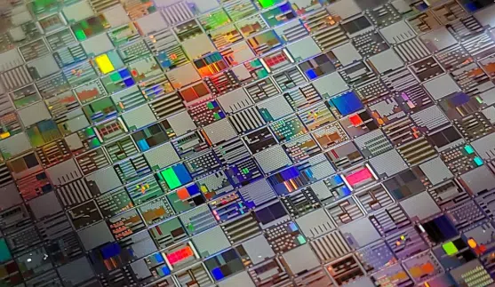
Wafer glass is a critical component in semiconductor, optics, and electronics manufacturing, serving as a substrate for thin-film deposition, optical coatings, and advanced packaging. Its applications span high-frequency circuits, MEMS devices, solar cells, and touch panels, requiring materials with tailored thermal, mechanical, and optical properties. As a specialized glass manufacturer, we provide custom wafer glass solutions in materials like BOROFLOAT® 33, PYREX®, Quartz,meeting stringent SEMI standards for precision and reliability.
In lighting, we can provide wafers of various materials to meet your requirements for different performances
Key Materials for Wafer Glass
Our high-purity glass materials are engineered for diverse industrial demands:
- BOROFLOAT® 33: A borosilicate glass with low thermal expansion and high thermal shock resistance, ideal for optical mirrors and high-temperature applications.
- PYREX®: Known for chemical durability and stability in harsh environments, suitable for semiconductor and LED packaging.
- Quartz /Fused Silica: Offers ultra-low thermal expansion and high UV transparency, critical for laser optics and lithography.
- EAGLE XG® :An alkali-earth boro-aluminosilicate glass with low CTE (~3.2×10⁻⁶/K), MEMS carrier wafers, and wafer-level packaging where thin, stiff, low-alkali substrates are required.
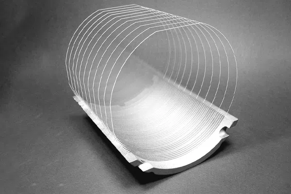
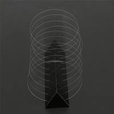
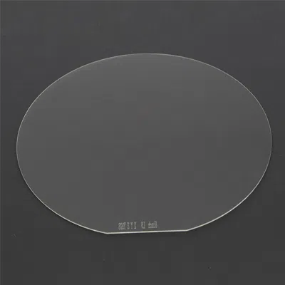
These materials are available in SEMI-standard sizes (2″ to 450mm) and custom geometries, with thicknesses as low as 25 microns and surface finishes from lapped opaque to optically polished.
Applications of Wafer Glass
Wafer glass supports cutting-edge technologies across industries:
- Semiconductor: Used as monitor wafers, dummy wafers, and interposers in 2.5D/3D packaging. Compatible with SOI (Silicon-on-Insulator) wafers and SiC (Silicon Carbide) wafers for high-power devices.
- Optics: Serves as substrates for custom optical components, including mirrors (e.g., Borofloat 33 with SiO₂-protected silver coatings for >98% IR reflectivity) and lithium niobate wafer modulators.
- Electronics: Enables LCDs, electroluminescent displays, and touch control panels with ultra-thin, scratch-resistant designs.
- Energy: Integral to solar cells and high-efficiency LED optics.
- Advanced Manufacturing: Supports MEMS, ceramic wafer coatings, and quartz wafer etching for precision sensors.
Custom Wafer Glass Fabrication Services
Our facility specializes in tailored solutions to meet unique specifications:
- Dimensional Customization: Produce wafers in diameters from 50mm to 450mm, with thicknesses ranging from 0.001″ (25 µm) to 3mm. Tight tolerances (±0.5 µm) ensure compatibility with wafer dicing, sawing, and thermal oxide processes.
- Surface Finishing: Options include optically polished edges (for low signal loss in high-frequency applications), chamfered edges, and SEMI-standard notches/flats.
- Post-Processing: Support wet cleaning processes (e.g., RCA cleaning for semiconductor-grade surfaces) and wafer cutting using laser or mechanical methods.
- Packaging: Secure wafer cassette packaging to prevent contamination during transport.
Support advanced wafer glass manufacturing workflow
We integrate with key industry processes:
- Semiconductor Cleaning: Our glass substrates are compatible with wet wafer cleaning tools (e.g., SC1/SC2 solutions) to remove particulates and organic residues.
- Wafer Dicing: Precision glass wafer dicing services minimize chipping, critical for sapphire wafers and silicon carbide wafers used in high-power electronics.
- Thermal Management: Materials like Quartz and BOROFLOAT® 33 exhibit low thermal expansion, reducing warpage in silicon wafer thermal oxide processes.
Why choose us as your wafer glass supplier?
As a glass factory in China with global reach, we combine advanced glass equipment manufacturing expertise with a vertically integrated supply chain:
- Material Diversity: Supply raw materials (e.g., PYREX® wafers, BOROFLOAT® 33wafers,EAGLE XG® wafer) and finished components.
- End-to-End Solutions: From custom optical components to ceramic wafer coatings, we streamline production for OEMs and suppliers.
- Quality Assurance: All products comply with SEMI standards, with certifications for surface flatness (<3 arcmin) and coating durability.
Order Custom Wafer Glass (2″–12″ & Panels)
We are a wafer glass supplier focused on high-purity substrates for MEMS glass substrates and wafer-level packaging glass. We stock and custom-make PYREX®/BOROFLOAT® 33, Quartz (fused silica), BK7, EAGLE XG®, D263T in SEMI sizes 2″–12″ (50–300 mm) and panels up to 600 × 800 mm with low TTV/warp, clean edges, and optical-grade polishing.
How to specify your order
- Diameter / panel size (2″–12″; custom on request)
- Thickness & tolerance (down to 25 μm where applicable)
- Surface finish (DSP / target Ra; scratch-dig)
- Flat/notch per SEMI; edge bevel/chamfer
- TTV/warp target (≤10 μm standard; ≤1 μm optional)
- Holes/slots/TGV (drawing with position tolerances)
- Coatings (AR, ITO, Cr/Au, hydrophilic/hydrophobic/AF)
- Quantity, packaging level (cleanroom cassette), and required lead time