

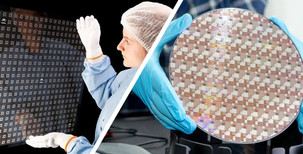
In the rapidly evolving world of Micro-Electro-Mechanical Systems (MEMS), the choice of substrate is a critical decision that influences a device’s performance, reliability, and cost. While silicon has long been the dominant material, glass wafers are increasingly becoming the substrate of choice for a wide range of MEMS applications. Their unique combination of properties—including optical transparency, electrical insulation, and superior chemical resistance—enables new functionalities and improves the manufacturing process.
This guide provides a comprehensive overview of glass wafers for MEMS, covering the materials used, the key fabrication processes, and the diverse applications where glass provides a distinct advantage.
What Are MEMS and Why They Matter
MEMS are microscopic devices that integrate mechanical and electrical components on a single chip. These systems can sense, control, and actuate on a micro-scale. Examples range from the accelerometers in your smartphone to the tiny micromirrors in a projector.
MEMS technology has revolutionized countless industries by enabling the creation of smaller, more efficient, and more powerful devices. The market is driven by the demand for sensors and actuators in consumer electronics, automotive safety systems, medical devices, and industrial automation. As MEMS devices become more complex and integrated, the need for advanced substrates that can support their intricate designs and demanding environments has never been greater.
Glass Wafers vs Silicon Wafers
While silicon is the workhorse of the semiconductor industry, and polymers are valued for their low cost and flexibility, glass offers a unique set of properties that make it a superior choice for specific MEMS applications.
| Feature | Glass Wafers for MEMS | Silicon Wafers |
| Optical Properties | Transparent from UV to IR. Essential for optical MEMS and imaging sensors. | Opaque in the visible spectrum. |
| Electrical Properties | Excellent electrical insulator. Prevents signal crosstalk and shorts. | Semiconductor. Requires complex insulation layers. |
| Thermal Properties | Low coefficient of thermal expansion (CTE) (e.g., borosilicate). Reduces thermal stress when bonded to other materials. | Low CTE, but can have mismatch with certain materials. |
| Chemical Properties | Highly resistant to harsh chemicals. Ideal for microfluidics. | Etches easily with common chemicals (e.g., KOH). |
| Cost | Generally more cost-effective for substrates of a specific purity and flatness. | Price can be high for high-purity, prime-grade wafers. |
For applications requiring optical transparency (e.g., optical MEMS), electrical isolation (e.g., RF MEMS), or chemical resistance (e.g., microfluidic glass chips), glass provides clear advantages. Its low CTE also makes it an ideal glass carrier wafer or interposer for handling fragile silicon devices during processing.
Glass Options for MEMS (Material Selection Guide)
The right choice of glass material is crucial for the success of a MEMS project. Each type of glass has a specific set of properties that make it suitable for different applications.
Borosilicate Wafer (e.g., BOROFLOAT® 33, Pyrex®, D263T):
Properties: This is the most popular choice for MEMS on glass. It has a low CTE, excellent chemical durability, and a high softening temperature. It is also well-suited for a key process called anodic bonding due to its specific alkali content.
Applications: Microfluidic chips, sensor covers, biomedical devices, and general MEMS substrates. D263T wafers are particularly popular for display and sensor applications due to their exceptional flatness and surface quality.
Fused Silica Wafer:
Properties: Made from high-purity silica, it has an extremely low CTE, superior optical transparency from the deep UV to the near-IR, and a very high working temperature.
Applications: Optical MEMS, high-temperature sensors, and applications requiring a low thermal budget. Its extremely low CTE makes it an excellent choice for a glass interposer or carrier wafer where thermal mismatch must be minimized.
Alkali-Free Glass (e.g., Eagle XG® Wafer):
Properties: Specifically engineered for display and electronics applications, it has a low CTE and is free of alkali ions, which can contaminate semiconductor devices.
Applications: Semiconductor packaging, display backplanes, and MEMS glass fabrication processes that are sensitive to ion contamination.
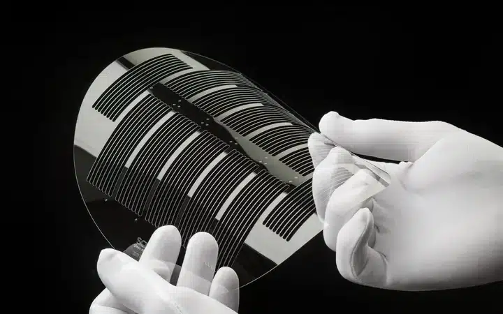
Core Processes on Glass (Patterning, Etching & Bonding)
Fabricating MEMS devices on glass requires specialized processes that differ from traditional silicon-based fabrication.
Glass Patterning:
This is the first step in creating features on the glass wafer. A thin layer of a photoresist material is applied and exposed to a light pattern.
Unlike silicon, which can be patterned using common photolithography, glass requires careful handling and specialized resist chemistries to ensure good adhesion and pattern transfer.
Etching:
Etching is the process of removing material to create features like channels, trenches, and holes. While wet etching can be used for some glass types, Inductively Coupled Plasma Reactive-Ion Etching (ICP-RIE) is the preferred method for high-aspect-ratio features.
ICP-RIE glass etch offers exceptional verticality and control, making it possible to create deep, precise features required for microfluidic glass chips and TGV (Through-Glass Via) interposers.
Bonding:
MEMS devices often consist of multiple layers bonded together.
Anodic bonding is the most common method for sealing a borosilicate glass wafer to a silicon wafer. This process uses heat and a high voltage to create a permanent, hermetic seal.
Glass frit bonding and thermocompression bonding are other methods used depending on the materials and application requirements.
Applications
The unique properties of glass wafers have enabled a new generation of MEMS devices:
- Microfluidics: Microfluidic glass chips are the backbone of lab-on-a-chip devices. Glass’s chemical inertness and optical transparency are ideal for handling biological fluids and performing optical detection of chemical reactions.
- RF MEMS: Glass wafers are excellent electrical insulators, preventing signal loss and crosstalk in high-frequency applications. They are used for RF switches, filters, and phase shifters.
- Optical MEMS: Glass is the perfect substrate for devices that manipulate light, such as micromirror arrays for projectors, optical switches, and variable attenuators. Fused silica wafers are a popular choice here due to their excellent transparency.
- Semiconductor Packaging & TGV: Glass interposers with Through-Glass Vias (TGVs) offer a cost-effective alternative to silicon interposers for 2.5D and 3D packaging. They provide electrical connections while offering superior mechanical stability and a more controlled CTE match with other components.
Our Glass MEMS Fabrication Capabilities
We specialize in precision MEMS glass fabrication, providing custom glass wafers, processing services, and full-scale manufacturing solutions. From material selection to final quality control, our team of experts ensures your project meets the highest standards.
- Custom Glass Wafer Supply: We source and supply a wide range of fused silica wafers, borosilicate wafers, D263T wafers, and Eagle XG® wafers, all precisely cut and polished to your specifications.
- Advanced Processing: We offer state-of-the-art services, including high-precision ICP-RIE glass etch for deep channels and TGVs, and advanced bonding services like anodic bonding.
- Prototyping & Volume Production: Whether you’re in the R&D phase or ready for mass production, we offer flexible services to scale with your project’s needs.
Contact us today to discuss how our expertise in glass wafers for MEMS can help you achieve your design goals and bring your innovative ideas to life.